GLOBALFOUNDRIES 7LP 7nm FinFET process technology platform
is ideal for high-performance, power-efficient SoCs in demanding,
high-volume applications.
3D FinFET transistor technology provides world-class performance,
power, area and cost advantages from 7nm scaling. 7LP technology
can provide more than 40% higher device performance and more
than 60% lower total power compared to 14nm technologies.
History:
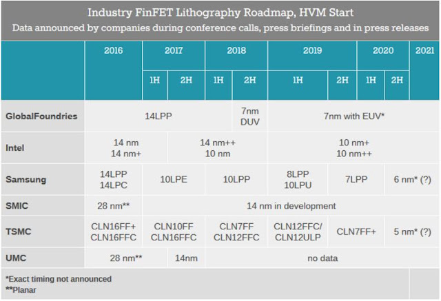
Over the past few years, companies like Samsung, TSMC, and GlobalFoundries have all jockeyed for the pole position in the highly competitive (and extremely expensive) foundry business. Even Intel, which used to march to the beat of its own drum, has gotten in on the action. As the cost of each new node has risen, the need to be first has increased as well. The first company to hit a new node tends to secure many of the most lucrative contracts. For most of the past two decades, the pure-play foundry world was dominated by TSMC, but Samsung beat its Taiwanese rival to 14nm and made a fair bit of cash in the process.
AnandTech Link for Roadmap of different companies: http://www.anandtech.com/show/11337/samsung-and-tsmc-roadmaps-12-nm-8-nm-and-6-nm-added
Overview By AnandTech:
Technology Overview:
• Twin-well CMOS bulk FinFET
• 5 Core device Vt’s
• Two gate dielectrics: thin (SG) and medium I/O (EG)
• Full suite of passive devices
• Optional MIM capacitor, eFuse
• VDD: 0.75V nominal or 0.85V overdrive
• Standard temperature range: -40°C to 125°C
• Optical lithography based process with EUV
compatibility
• Up to 17 layers of metallization
Performance, Power, Cost Advantage
from 7nm Area Scaling :
>40% performance improvement at iso power (vs. 14nm)
>60% power reduction at iso frequency (vs. 14nm)
Up to 30% lower die cost (vs. 14nm)
Application-optimized Platform Extensions:


Comments
Post a Comment